Dec 11, 2024
Dec 10, 2025
Products
Challenges and Advancements in Semiconductor Chip Picking
In this article, we’ll start with a simple overview of the processes and machines involved in making semiconductor chips and the products all around us that rely on them. We’ll then take a closer look at some of the challenges that arise in the semiconductor chip picking process, where chips are grabbed and lifted. After that, we’ll suggest methods for damage control using THK’s Pick and Place Robot (PPR) by sharing examples of user challenges and product applications.
We hope that young engineers just entering the semiconductor industry as well as veterans who are already grappling with the challenges of the chip picking and placing processes find this article useful.
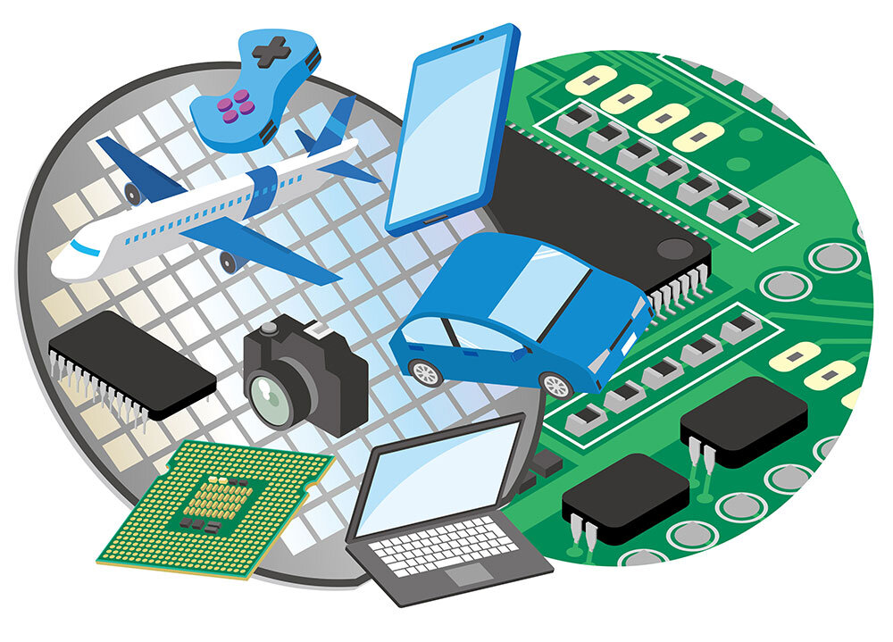
Semiconductors, the “Bread and Butter of Industry”
Semiconductors have been called the “bread and butter of industry,” but just how ubiquitous are they really?
Let's start with CPUs. Inside the smartphones and computers that we have with us everywhere we go is an information processing and calculation device called a CPU. While you might think that any given device would only have a single CPU, in reality, many modern computers have multiple built-in CPUs like quad-core processors for handling large quantities of data. And there are many examples of systems with multiple CPUs processing information independently, with each dedicated to a specific function. Some vehicles are outfitted with 30 CPUs or more, for example.
Next, let's look at storage space, or memory drives. CPUs can process information, but they can’t store it. If performing a calculation caused the result of the previous calculation to disappear, though, nothing would ever get done. Memory drives are the devices that store data temporarily or long-term while large amounts of information are being processed.
And what about sensors? Take image sensors, for instance. Image sensors are used in things like smartphones and digital cameras. They capture external point and color information, which is converted into data. This data is then processed into a form that can be treated as a picture or an image file. Image sensors, as well as photosensors, acceleration sensors, and pressure sensors, play a big role in making our lives safer and more prosperous.
Last but not least, let's look at LEDs. Semiconductors have also revolutionized the way that we light the spaces we're in. LEDs have rapidly replaced conventional incandescent and fluorescent lights thanks to their high luminescence, long life, low energy consumption, and compact size. They are used to light everything from cars, traffic signals, and streetlights to smartphone and monitor displays.
Considering all of these applications for semiconductors, it’s easy to see how indispensable the “bread and butter of industry” really is for our lives.
Semiconductor Chips and their Manufacture
How are semiconductor chips made, though?
First of all, semiconductors are made of a silicon-based material.1 Ingots of monocrystalline silicon are cut into wafers before pre-processing that includes patterning and die singulation, where the wafer is further broken up. This produces semiconductor chips, which are also called dies. The term “chip” refers to the way these parts are flecks or fragments of the larger silicon ingot. “Die,” on the other hand, means a square of material or a cube like those used in board games. This is the “die” in the name of the die singulation process.
At this point, even though the silicon material is cut into individual dies, these alone can’t be mounted to any kind of circuit.2 Dies must be mounted to a polarized lead frame or semiconductor package that is itself in contact with a given circuit. This process is called die bonding. Here, the die is fixed in place by either soldering or through the use of an adhesive. During the next process, called wire bonding, the die is connected to the lead frame or semiconductor package using fine metal wires. These wires, and the surface of the semiconductor chip itself, are still exposed at this stage and require delicate handling. To lend them some additional durability, resin is poured out to form a protective capsule over them during the next process, known as molding.
1 Other materials are also used.
2 A technique called “flip chip bonding” also exists at time of writing.
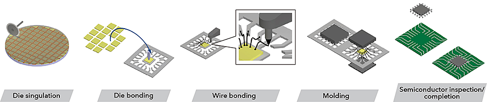
Among the various machines that are used in these processes are dicers for die singulation, die bonders for setting dies (chips), sorters for organizing dies prior to die bonding,* and wire bonders for wire bonding.
* Sorters can remove chips determined to be defective during testing.
Challenges in Picking Up Semiconductor Chips
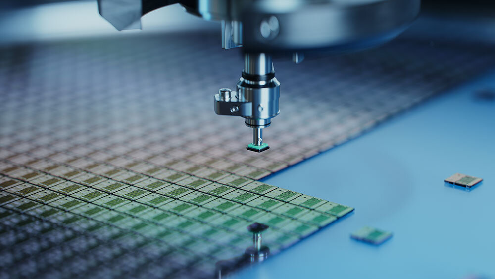
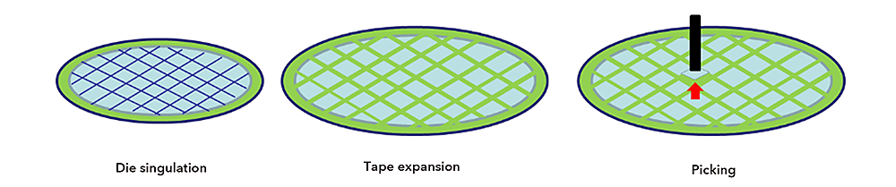
Let’s return to the processes where wafers are broken into individual chips and these chips are picked up. During die singulation, wafers are stuck to adhesive tape to prevent chips from scattering when they are cut. Afterwards, the chips cut from the wafer are grabbed by a picking tool and removed from this tape. The physical properties of silicon make it easy to break or crack the material with even a small impact. This poses the risk of damaging chips that have already made it through pre-processing. To avoid this, the adhesive tape stuck to the wafer is expanded, and ejector pins are used to lift individual chips from below. This makes it easier for picking tools to then remove each chip from the adhesive tape.
Using ejector pins to lift chips makes it easier to remove them from the adhesive tape, but it requires highly advanced technology. Below are some factors that complicate this process.
- Chips are very thin and very delicate
- Ejector pins and picking tools must move in sync with each other
- Wear can change the relative positions of ejector pins and collets* with respect to the chips
* In the semiconductor and electronic component industries, a suction nozzle is called a collet.
Let's look at each of these complicating factors more closely.
1. Chips are very thin and very delicate.
As mentioned above, ingots are sliced into thin pieces to produce semiconductor wafers. Making these wafers thin means that a single ingot can yield more of them, which drives down the cost of each. And the smaller and thinner semiconductor devices are, the less area and volume they require when mounted to a circuit board. All of this contributes to making the finished electrical device more compact and making the final product easier to use. While many chips are cut to a width of 0.5 mm to 1.0 mm for the sake of making them harder to break and thus easier to handle, some cutting-edge chips can be as thin as 20 μm.
2. Ejector pins and picking tools must move in sync with each other.
Ejector pins are driven upward from beneath a semiconductor wafer by a servomotor or other system. Collets attached to picking units are also driven by servomotors and similar systems, though they are driven downward. The sequence of events for picking up a semiconductor chip is:
1. The collet is lowered to make contact with the chip. (Air suction is applied at this time.)
2. The ejector pin is raised.
3. The ejector pin and collet are raised at the same time.
4. The collet continues to rise, picking up the chip.
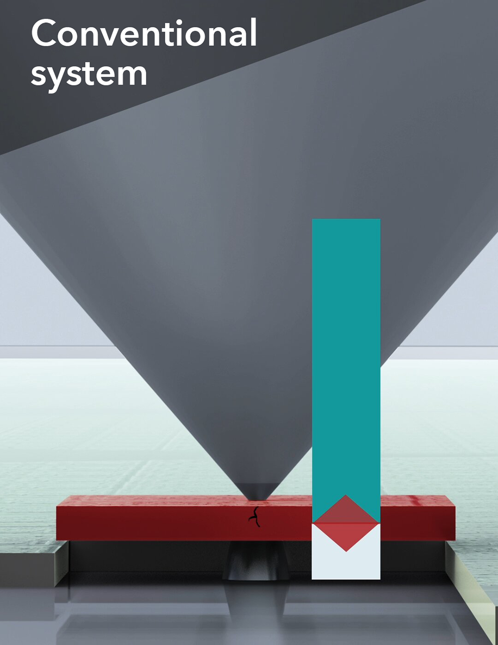
During this process, the chip is subject to impacts from both the collet and the ejector pin making contact with it as well as from being pinched between them. Reducing the damage done to these thin semiconductor chips requires a high level of position control, speed control, and synchronized motion along the vertical axis. According to our research, pinching of just a few dozen microns applies a load in the hundreds of grams, making strict position control essential.
3. Wear can change the relative positions of ejector pins and collets with respect to the chips.
Ejector pins and collets make contact with chips thousands if not tens of thousands of times each day, which can gradually wear them down. In order to prevent this wear, cemented carbides and even diamonds are used to make these components. All the same, the tips of these components can become warped such that their relative positions with respect to the chips are altered, which can cause ejection errors as well as damage to the chips being handled.
The PPR System and the Improvements It Offers
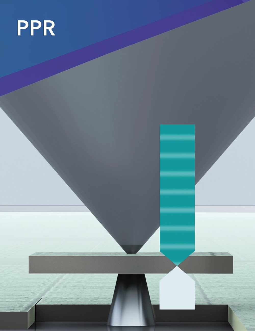
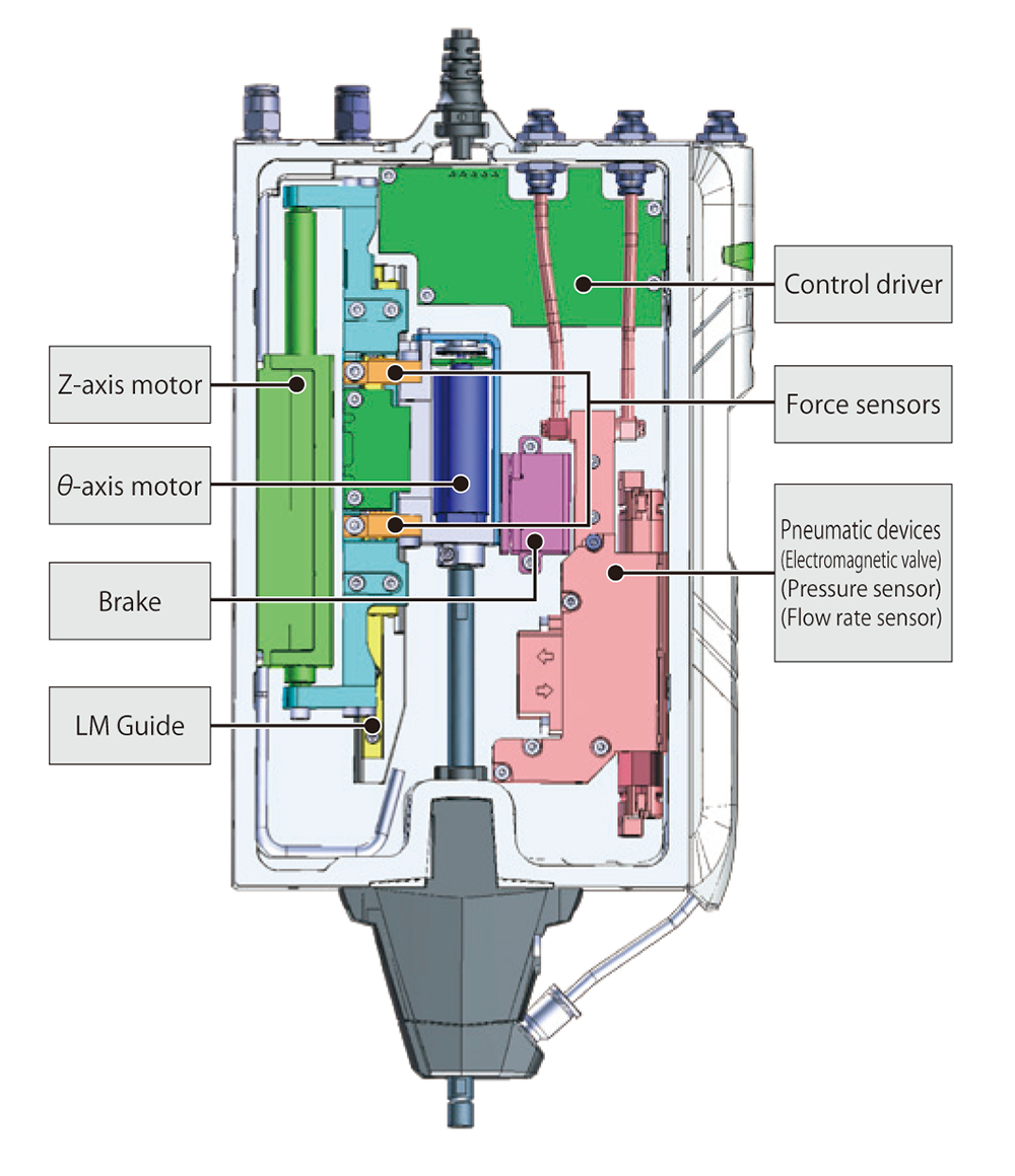
As an all-in-one system, the PPR comes with a built-in linear motor and encoder for the Z axis and a force sensor. It is the tool of choice for a wide array of semiconductor chip picking processes.
With a contact stop function that activates as soon as the collet touches the semiconductor chip , the PPR reduces the impact that the chip receives. This same function can also prevent fluctuations in the intensity of this kind of impact that might occur as a result of collet displacement caused by wear. Also, because the PPR is capable of detecting position information down to the micron, it can even detect such collet wear by checking the collet’s position when it makes contact with the chip.
See this page for a case study of a proposed solution in which height determinations are made using position information.
Using the PPR's pressing force control function for synchronizing with ejector pins makes it possible to maintain a set load applied to chips being picked up. This in turn prevents impacts that exceed that set load when chips are lifted, even if motion along the vertical axis isn’t synchronized with a high degree of accuracy.
See this page for a case study of a proposed solution that shows the behavior of force sensors used for pressing force control.
Supporting Increased Yields from Semiconductor Manufacturing Processes
This time, we turned our attention to how semiconductor chips are picked up during processing. We covered challenges around damage control as well as process improvements made possible by the Pick and Place Robot PPR. As mentioned in the first part of this article, semiconductors are indispensable to the world, and if we are to expect ever greater functionality from things like the smartphones we carry with us wherever we go, semiconductors must become ever smaller and thinner. From what users of our products tell us, though, we get the impression that a multitude of equipment and device manufacturers are struggling with this very thing.
We believe that the PPR and THK's other technologies will continue to help our customers overcome their challenges and generate new breakthroughs for the semiconductor industry, so please don’t hesitate to reach out to THK for support.
Product Blog: Optimal for Suction Transfer Processes in Crystal Oscillator Manufacturing! The Functionality of the Pick and Place Robot (THK website)
The World's First Process-Optimizing Robot: Pick and Place Robot (THK website)
* This content is based on information that was released in Japanese on December 11, 2024.